Microelectronics | 80386DX ISA SINGLE BOARD MICROCOMPUTER
Synopsis
Living in the early 1990s, along with the technological advancements in computing and microelectronics, was a rewarding experience. While I initially had little access to the latest technologies, everything shifted with the beginning of the decade. By chance, I had the opportunity to own a very high performance computer for the time being. It was an 80386SX CPU-based machine, running at 25 MHz. Further equipment included 2 Mb RAM, integrated AcuMOS AVGA2 card with 256 K graphics memory, and a 40 Mb Seagate hard disk drive. All packed in a Kenitec branded desktop case and connected to a 12" AOC monochrome VGA monitor. I discovered modern operating systems, games, and -- drum roll, please -- computer programming. This is the context that marked my life in terms of computers. It changed it completely, shifting my perspective to 180 degrees.
But let's put history aside for a moment and let's concentrate on the motivation. Why would somebody ever attempt to build a vintage computer system? Let alone design one from scratch in 2019? This is over 30 years old technology that is now pretty much useless. All period correct computer software can be now run in software emulators, on any platform. Mobile phones have tremendous computing power. Tablet computers dominate the mobile market. Then, why build such a thing? The answer could be very biased. Let's say nostalgia and -- why not? -- because of the engineering challenges. Sure, I can buy any 80386DX based mainboard from the big auction site. But it would be better if I'd (sic) built it myself.
Let's dig into the specifications and my choice of components then.
Hardware Specifications
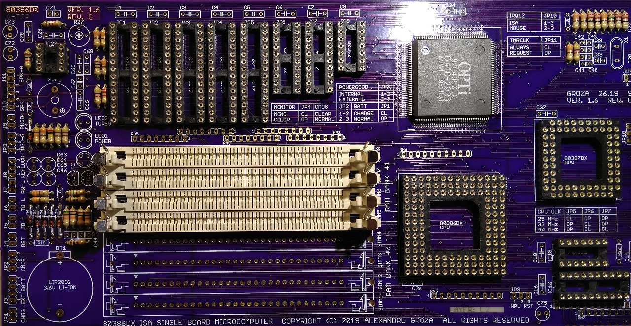
- 32-bit 80386DX CPU
- 32-bit 80387DX NPU
- 128 K Cache System
- 32 Mb RAM (16 Mb RAM in BANK0 and 16 Mb RAM in BANK1)
- Standard 80386DX AMI BIOS
- 8042-class PS/2 Keyboard and Mouse Controller
- OPTi Chipset (82C495XLC and 82C206)
- Port 80h On-board Diagnostics
- Minimal Glue Logic
- Individual hardware configuration switches and jumpers for all functions
- 16-bit ISA-class printed circuit board construction
These are the main specifications of this system design. I decided to go with a simple approach, using a verified design solution based on an OPTi chipset. This reduces the integrated circuit count, power consumption, and eventual connection wiring design errors. Also, a smaller ISA card footprint translates into smaller fabrication costs -- which unfortunately are expensive anyway. I tried to stay away from surface mounted parts as much as I could, for a period correct look. However, the 82C495XLC system control chip comes only in PQFP-160 package. That is a lot of pins to solder.
The schematic diagram that I produced is the result of about one month of sustained work. In order to accomplish this design, I thoroughly studied the following documents.
- Intel 80386DX Datasheet
- Intel 80387DX Datasheet
- OPTi 82C495XLC Datasheet
- OPTi 82C206 Datasheet
- VIA VT82C42 Datasheet
- ISA-bus Specifications and Pinout
- SIMM Design and Pinout Documentation
I couldn't find any available datasheet for some electronic parts involved in this system design. I got to know them because I have seen them being used on a lot of mainboards of the era. This calls for reverse engineering as it is the only way I could accomplish the schematic diagram. How I did it? I bought three or four generic 80386DX boards from the local flea market and observed the connections and layout. It was a tedious work and it accounted for most of the time spent designing this microcomputer. I hand-drew all these mini-schematics on paper, and analyzed them by comparison to existing designs published in technical literature such as Integrated Circuit Systems Data Book, 1995 edition. And other similar data books and system design literature that I have. Low-level programming background also helped a lot while working with address and data signals. I don't claim that the produced design is entirely correct but it is the best I could do. Sometimes, I just used my electrical engineering knowledge and engineering common sense to design and interconnect the modules. In the end, I have translated everything into a CAD program. Oh, not to mention that I routed all the ~8,400 wires, by hand, on a four layer printed circuit board. Computer assisted design software has become a serious performer but, in certain cases, the human brain far exceeds the capabilities of any existing software to date. At least this is what I like to believe...
It is worth mentioning that the PCB that I designed is a little bit longer than the maximum allowed length for ISA cards. It will not fit shallow computer cases. So a slightly deeper case is required to accommodate the SBMC card.
In addition, the following work was carried in order to design this microcomputer.
- Reverse Engineering of Wiring on HM8226
- Reverse Engineering of Wiring on IMI SC425APB
- Reverse Engineering of Wiring on Interfacing Cache Memory Banks
- Reverse Engineering of Wiring on PS/2 Keyboard and Mouse Controller Interface
- Reverse Engineering of ISA-bus Arbitration Signaling
I would also highly recommend the ISA System Architecture book by Tom Shanley and Don Anderson. A lot of valuable information can be found within those pages.
In the end, I should say that I have seen a lot of computer hardware over the time and I have also low-level repaired such hardware. Thus, I am quite familiar with the x86 architecture.
Some parts of the schematic are optional. The system can run as expected without them. I am referring here to the Port 80h On-Board Diagnostics section, buffered PC Speaker output circuit, external battery support, 3.6 V LIR2032 lithium-ion battery charging circuit, Power Good internal signal generation, PS/2 mouse interface, and some jumpers. Sure the electrical schematic diagram can be reduced, and the printed circuit board can simply omit these parts. Also jumpers can be hardwired. But I wanted to experiment a little bit so that I can expand my own knowledge. And we all know how much we'd wanted our PCs to be maxed out (i.e.: all IC sockets populated, maxed RAM and cache, NPU present, and fastest CPU speed setting).
Sourcing components for this project is not that hard at all. CPU, NPU, OPTi chips, ROM BIOS, and Keyboard controller can all be acquired from auction sites. HM8226 and IMI SC425APB as well but you need to be patient to find them. Alternatively, you can carefully rescue these from existing (dead, or not) PCBs. Just like I did. ROM BIOS can also be freely downloaded from the Internet and burned into an UV-erasable EPROM integrated circuit of the right internal organization. You just need to make sure you find the right 80386DX 64K ROM BIOS image. The rest of the components are available at Mouser. I will add a bill of materials (BOM) down below for references. Printed circuit board can be ordered at OSHPark. It is expensive but build quality is high. You will find a link to the project in the BOM below.
Later Edit: Originally, I wanted this page to be a simple presentation of my work. But it slowly morphed into this giant wall-of-text describing my research, issues, resolutions, and conclusions in the field of x86 microcomputer system design.
Disclaimer: I reserve the right to change the schematic diagram, the PCB layout, or the implementation without further notice. This is an entirely hobby do-it-yourself design and I am not responsible for any damage made by any possible mistake in any version or revision of the schematic diagrams or PCB layouts. Since it is an advanced microelectronics project, it requires very good assembly and debugging skills. In addition, I cannot offer any further technical support other than the contents of this article.
This project is in its final stage.
Current iteration of ASSY. 2486-SBMC-101 is VER. 1.8 REV. E
* * *
Laudatur ab his, culpatur ab illis. This project is provided as-is and is not for commercial purposes. It reflects my experimental work in microcomputer system design and should be treated as such. I release the schematic diagram and circuit board layouts to the public for educational purposes. I did all this at my own expense and in my free time. If you like my work, please consider making a donation. It helps me continue these kind of projects.
Schematic Diagram (VER. 1.8 REV. E)

Fig. 1: Electrical Schematic Diagram
Printed Circuit Boards (VER. 1.8 REV. E)

Fig. 2: Top Silkscreen

Fig. 3: Top Layer Printed Circuit Board

Fig. 4: Inner Bottom Layer Printed Circuit Board

Fig. 5: Inner Top Layer Printed Circuit Board

Fig. 6: Bottom Layer Printed Circuit Board

Fig. 7: Top Layer Printed Circuit Board - Simulation

Fig. 8: Bottom Layer Printed Circuit Board - Simulation
If you want to see or hide older schematic diagrams, please use the following function: Show Older Schematic Diagrams


Gerber Files
Here are the Gerber files compressed in a .ZIP archive.
Please note that the file naming convention that I used is what OSHPark normally expects.
You can also order the printed circuit board directly from OSHPark by following the link in the bill of materials below.
Compressed Gerber Files: isa-80386dx-sbmc.zip
Bill of Materials (BOM)
The following list contains the parts that are required to assemble this microcomputer.
| 80386DX ISA SINGLE BOARD MICROCOMPUTER | ||||
|---|---|---|---|---|
| Identifier | Value | Qty | Notes | Mouser Number |
| Printed Circuit Board | ASSY. 2486-SBMC-101 | 1 | VER. 1.8 REV. E | Order from OSHPark |
| IC1-IC4 | 61C256AH-20 | 4 | 256 Kbit SRAM | Order from 3rd Parties |
| IC5 | 61C64AH-20 | 1 | 64 Kbit SRAM | Order from 3rd Parties |
| IC6 | 74ACT373 | 1 | Octal 3-state D Latch | 595-SN74ACT373N |
| IC7, IC15 | 74F244 | 2 | Octal 3-state Buffer | 595-SN74F244N |
| IC8, IC27 | 74F08 | 2 | Quad 2-input AND Gate | 595-SN74F08N |
| IC9 | 27C512 80386DX ROM BIOS | 1 | 512 Kbit ROM | 556-AT27C512R70PU |
| IC10-IC17 | 74LS245 | 7 | Octal Bus Transceiver | 595-SN74LS245N |
| IC18 | 74F125 | 1 | Quad 3-state Buffer | 595-SN74F125N |
| IC19 | 74LS32 | 1 | Quad 2-input OR Gate | 595-SN74LS32N |
| IC20 | 74ALS574 | 1 | Octal D Flip-Flop | 595-SN74ALS574BN |
| IC21 | 74LS688 | 1 | Magnitude Comparer | 595-SN74LS688N |
| IC22, IC23 | DM9368 | 2 | 7-segment Decoder | Order from 3rd Parties |
| IC24 | 74LS07 | 1 | Hex Buffer (OC) | 595-SN74LS07N |
| IC25 | 74ALS04 | 1 | Hex Inverter | 595-SN74ALS04BN |
| IC26 | 74F32 | 1 | Quad 2-input OR Gate | 595-SN74F32N |
| IC28 | SC425APB | 1 | Clock Generator | Order from 3rd Parties |
| IC29 | LM386 | 1 | Audio Amplifier | 926-LM386N-1/NOPB |
| IC30 | AMI KB-BIOS-VER-F | 1 | Keyboard Controller | Order from 3rd Parties |
| IC31 | HM8226 | 1 | Order from 3rd Parties | |
| IC32 | 74LS06 | 1 | Hex Inverter (OC) | 595-SN74LS06N |
| IC33 | CD4069 | 1 | CMOS Hex Inverter | 595-CD4069UBE |
| IC34 | OPTi 82C495XLC | 1 | System Controller | Order from 3rd Parties |
| IC35 | OPTi 82C206 | 1 | Peripheral Controller | Order from 3rd Parties |
| IC36 | Intel A80386DX-33 IV | 1 | CPU | Order from 3rd Parties |
| IC37 | Intel A80387DX-33 | 1 | NPU | Order from 3rd Parties |
| IC38 | MCP73831 | 1 | Battery Management | 579-MCP73831T-2ACIOT |
| T1 | 2N3906 | 1 | Small Signal Transistor | 512-2N3906BU |
| T2 | 2N3904 | 1 | Small Signal Transistor | 512-2N3904BU |
| T3 | 2N2222 | 1 | Small Signal Transistor | 610-2N2222 |
| D1-D5 | 1N4148 | 5 | Small Signal Diode | 78-1N4148 |
| C1-C37, C82-C85 | 100 nF / 50 V | 42 | MLCC | 80-C322C104M5R-TR |
| C38-C39, C40-C43 | 10 pF / 50 V | 6 | MLCC | 80-C315C100J5G |
| C44 | 470 pF / 50 V | 1 | MLCC | 80-C315C471K5R |
| C45, C71 | 47 nF / 50 V | 2 | MLCC | 80-C320C473K5R |
| C46, C63-C65 | 1 uF / 35 V | 4 | Tantalum Capacitor | 80-T350A105K035AT |
| C47-C50, C54-C57 | 47 pF / 50 V | 8 | MLCC | 80-C315C470J5G |
| C51, C52, C58, C59 | 56 pF / 50 V | 4 | MLCC | 80-C315C560J5G |
| C53, C60, C66, C68 | 100 nF / 50 V | 4 | MLCC | 80-C322C104M5R-TR |
| C61, C62 | 220 pF / 50 V | 2 | MLCC | 80-C315C221K5R |
| C67 | 2.7 nF / 50 V | 1 | MLCC | 80-C315C272K5R |
| C72 | 220 uF / 6.3 V | 1 | Polymer Capacitor | 80-A758BG227M0JAAE18 |
| C73, C86-C97 | 10 uF / 25 V | 13 | Tantalum Capacitor | 80-T350E106M025AT |
| C74 | 100 pF / 50 V | 1 | MLCC | 80-C315C101K5R |
| C75 | 22 pF / 50 V | 1 | MLCC | 80-C315C220J5G |
| C76, C77 | 4.7 uF / 50 V | 2 | MLCC | 80-C322C475K5R |
| C69, C70, C78-C80 | 10 uF / 25 V | 5 | MLCC | 80-C322C106K3R |
| C81 | 100 nF / 50 V | 1 | MLCC | 80-C320C104M5R |
| C98 | 1 nF / 50 V | 1 | MLCC | 80-C315C102F5G |
| C99-C101 | 10 nF / 50 V | 3 | MLCC | 80-C315C103J5R |
| R1, R25 | 47 kΩ | 2 | Carbon Resistor | 291-47K-RC |
| R2, R28, R29, R31, R38 | 1 kΩ | 5 | Carbon Resistor | 291-1K-RC |
| R3, R5 | 10 kΩ | 2 | Carbon Resistor | 291-10K-RC |
| R4 | 51 kΩ | 1 | Carbon Resistor | 291-51K-RC |
| R6 | 2 MΩ | 1 | Carbon Resistor | 291-2M-RC |
| R7, R8, R36, R44, R45 | 470 Ω | 5 | Carbon Resistor | 291-470-RC |
| R9, R10, R15, R42 | 150 Ω | 4 | Carbon Resistor | 291-150-RC |
| R11-R14 | 22 Ω | 4 | Carbon Resistor | 291-22-RC |
| R16, R17, R20, R22 | 330 Ω | 4 | Carbon Resistor | 291-330-RC |
| R18, R23 | 33 Ω | 2 | Carbon Resistor | 291-33-RC |
| R19 | 100 Ω | 1 | Carbon Resistor | 291-100-RC |
| R21 | 200 kΩ | 1 | Carbon Resistor | 291-200K-RC |
| R24 | 2.2 kΩ | 1 | Carbon Resistor | 291-2.2K-RC |
| R26, R37 | 4.7 kΩ | 2 | Carbon Resistor | 291-4.7K-RC |
| R30 | 51 Ω | 1 | Carbon Resistor | 291-51-RC |
| R32-R35, R39-R41, R43 | 330 Ω | 8 | Carbon Resistor | 291-330-RC |
| R27 | 10 kΩ | 1 | Trimmer Resistor | 72-T7RYA103KT20 |
| RN1-RN5 | 9 x 4.7 kΩ | 5 | Bussed Resistor Network | 652-4610X-1LF-4.7K |
| RN6 | 9 x 1 kΩ | 1 | Bussed Resistor Network | 652-4610X-1LF-1K |
| RN7, RN8 | 7 x 2.2 kΩ | 2 | Bussed Resistor Network | 652-4608X-1LF-2.2K |
| RN9-RN11 | 7 x 4.7 kΩ | 3 | Bussed Resistor Network | 652-4608X-1LF-4.7K |
| RN12 | 4 x 4.7 kΩ | 1 | Bussed Resistor Network | 652-4605X-1LF-4.7K |
| RA1-RA5 | 4 x 22 Ω | 5 | Resistor Array | 652-4608X-2LF-22 |
| L1-L10 | BL03RN2 | 10 | Ferrite Bead | 81-BL03RN2R1P1A |
| X1 | 14.31818 MHz | 1 | Quartz Crystal | 695-HC49US-143-U |
| X2 | 32.768 kHz | 1 | Quartz Crystal | 695-CFS-20632768DZBB |
| F1 | 1.1 A / 16 V | 1 | Resettable Fuse | 576-16R110BU |
| DISP1, DISP2 | RFT VQB37 | 2 | Common Cathode | Order from 3rd Parties |
| LED1 | 5 mm Green LED | 1 | Power Indicator | 755-SLR-56MC3F |
| LED2 | 5 mm Orange LED | 1 | Turbo Indicator | 755-SLR-56DC3F |
| LED3 | 5 mm Green LED | 1 | Charged Indicator | 755-SLR-56MC3F |
| LED4 | 5 mm Orange LED | 1 | Charging Indicator | 755-SLR-56DC3F |
| IC Socket | 28-pin | 5 | IC1-IC5 | 575-11043328 |
| IC Socket | 20-pin | 12 | IC6, IC7, IC20, IC21, IC10-IC17 | 575-193320 |
| IC Socket | 14-pin | 10 | IC8, IC18, IC19, IC24-IC28, IC32, IC33 | 575-193314 |
| IC Socket | 16-pin | 2 | IC22, IC23 | 575-110433161 |
| IC Socket | 28-pin | 1 | IC9 | 575-11043628 |
| IC Socket | 8-pin | 2 | IC29, IC31 | 575-193308 |
| IC Socket | 40-pin | 1 | IC30 | 575-193640 |
| IC Socket | 84-pin PLCC | 1 | IC35 | 575-948424 |
| IC Socket | 132-pin | 1 | IC36 | 575-510-313214 |
| IC Socket | 68-pin | 1 | IC37 | 437-5108706811061101 |
| SIMM Socket | 30-pin | 8 | SIMM1-SIMM8 | Order from 3rd Parties |
| SPK1 | Electromagnetic Speaker | 1 | 85 dBA | 665-AT-1224TWTR |
| Battery Holder | *2032 | 1 | BT1 | 122-2420-GR |
| JP1, JP4-JP7, JP11, JP12 | 2-pin Header | 7 | Jumper | 649-68001-202HLF |
| JP2, JP3, JP8-JP10 | 3-pin Header | 5 | Jumper | 649-68001-203HLF |
| J3, J10 | 4-pin Header | 2 | Header | 649-68001-204HLF |
| J4-J7, J9, J11 | 2-pin Header | 6 | Header | 649-68001-202HLF |
| J8 | 3-pin Header | 1 | Header | 649-68001-203HLF |
| J1 | 6-pin Mini DIN Connector | 1 | PS/2 Keyboard | 571-5749265-1 |
| J2 | 6-pin Mini DIN Connector | 1 | PS/2 Mouse | 571-5749265-1 |
| H1, H2 | 16-pin IC Heat Sink | 2 | Optional for IC22, IC23 | 567-651-B |
| H3 | 37 x 37 x 4 IC Heat Sink | 2 | Optional for IC36 | Order from 3rd Parties |
| ISA Card Bracket | Custom Built | 1 | 3D Printed | N/A |
Alternatively, you can use the following link to the Mouser project that I created for this microcomputer. It should make ordering of parts and removing typing faults pretty easy.
Mouser Project: 80386DX ISA SINGLE BOARD MICROCOMPUTER
Lately, I have observed that Mouser discontinued some of the parts in the list above. If you decide to build this project, then you need to find alternatives. It is out of my scope to maintain the correctness of the parts list above.
Notes:
- 61C64 and 61C256 are available at Mouser but not in the right package. Either you build an ugly and dirty adapter or you source the SRAMs in the required package from electronic parts auction sites.
- TTL ICs need to be of Low-power Schottky (LS) type with a typical gate delay of about 10 ns. In some key places in the schematic I went for Advanced Schottky (74F) series parts with a typical gate delay of about 1.7 ns.
- In place of the LS series ICs you can also use 74ALS, 74HCT, 74ACT, or 74AHC series parts. In place of the F series ICs you can use 74FC parts. For bus driving transceivers, I would stick to 74LS series since they have hysteresis capabilities on their inputs.
- 27C512 UV-erasable EPROM is required. I always found these kind of ICs to be looking very nice.
- 80386DX ROM BIOS image that I used is inscribed inside an original AMI BIOS integrated circuit. You can either source a compatible original AMI ROM BIOS integrated circuit or find a binary image on the Internet. Then you need to burn it into a 27C512 UV-erasable EPROM integrated circuit. Refer to 80386DX ROM BIOS section down below for more information.
- DM9368 decoders are mandatory for the Port 80h On-Board Diagnostics circuit. Sure, other decoder ICs could -- and should partially -- work but DM9368 have internal current limiting resistors for the 7-segment elements. I went for this approach in order to reduce parts count. These ICs are running quite hot so optional heat sinks can be used to cool them down.
- SC425APB can be replaced with standard integrated metal-can oscillators. Although this approach would have made for a simpler parts sourcing procedure, it would have increased parts count in order to support multiple CPU clocks. If you don't succeed sourcing a SC425APB master clock generator then just build an adapter. Read the SC425APB Replacement section for more information.
- IC25, part of the reset circuit, must be of type 74ALS04. As a side note, plain 7404 TTL parts will work as well. Even though I specified IC25 of type 74LS04 in schematic diagram revisions prior to REV. E, in practice, I always went with a 74ALS04 IC instead.
- You absolutely need an AMI KB-BIOS-VER-F keyboard controller in order to make use of PS/2-mode with the AMI BIOS dated 8/8/93. However, other BIOSes can use different keyboard controllers. For instance, VIA VT82C42, which is readily available on multiple sources. Or other PS/2 capable keyboard controllers ICs such as HT6542B. I think you can also use one of the original 8242 microcontrollers. But you need to source one with PS/2 compatible software written inside.
- If you don't find the Hualon Micro HM8226 integrated circuit then just install jumper in position JP11.
- I have recovered the 82C495XLC from a working 80386DX mainboard. I have seen a lot of 82C495XL parts on eBay but I don't know what is the difference between the ones with the C suffix and the ones without it. They might work as well in this system design but I have no way to prove this theory.
- Instead of OPTi 82C206, I have initially used a Siemens SAB82C206N part. This came with a cheaper transportation fee than the OPTi chip. Then I found a pack of three CHIPS P82C206 integrated circuits that I bought cheap.
- Ferrite beads are used to reduce electromagnetic noise on digital and analog transmission lines. Sure, the circuit will work without them as well but it is better to be on the safe side. Less circuit debugging is better.
- I chose to use the miniature bubble displays made by RFT because I have a box full of them, all NOS. These seldom appear on eBay. And while not as readable as conventional 7-segment displays, they sure look nice enough to be used in such a project. The deep red color is nice to observe, nonetheless.
- The coin cell battery must be of LIR2032 type since these can source 3.6 V instead of the most common 3 V for CR2032 batteries. The reason for this choice is the added diode in series with the battery. This approach ensures an additional 0.7 V drop so battery voltage seen by 82C206 is about 3 V. In case of the 3 V battery, the voltage seen by this IC would've been too low, peaking at about 2.3 V. However, the first PCB revision had some issues with the charging circuit. Lithium-ion batteries are normally charged through a strictly controlled process. The original, very basic charger with a resistor in series, was more suitable for charging NiMH batteries. Of course, the LIR battery could be charged as well but it would've been a risky approach. Using such a simple circuit would require careful observation of the cell temperature while charging. Lithium-ion batteries can burst in flames in a split second, damaging the board and possibly injuring you. The first PCB revision would've been far better to be used with the 6 V external battery pack, only.
- If you decide to go for a 40 MHz system clock, I would recommend to use small heat sinks on both the CPU and the NPU.
- For the ISA card bracket, I went for a custom 3D printed one. Sure, I could've adapted an existing bracket but building one to the exact requirements of this board would be better. Refer to 3D Printed ISA Bracket section down-below for more information.
Assembly Instructions and Notes
Here is a list of things you need to pay attention to should you decide to build such ISA single board microcomputer.
- Inspect the printed circuit board once you receive it. Normally OSHPark produces very good quality boards but one never knows. There must be absolutely no short circuits on the printed tracks. If the PCB is faulty then it can damage valuable electronic components and other ISA cards that you might install in the system.
- Carefully observe polarity of the tantalum electrolytic capacitors on the silkscreen. I made sure there is no error on the printout so even if it appears weird, please do respect the markings. Tantalum capacitors will violently explode and burst in fire if mounted in reverse, possibly injuring you.
- Take your time to solder all the components on the board. There are a lot of solder points and if you don't have patience in general, then this project might not be for you.
- Use a temperature-controlled soldering station and quality solder. Take care not to leave solder bridges as any short circuit will most likely lead to failures.
- In order to ease-up the PCB assembly, I would suggest mounting parts in the following order: OPTi 82C495XLC, diodes, resistors, ferrite beads, quartz crystals, 7-segment displays, IC sockets, resistor networks, transistors, MLCC capacitors, tantalum capacitors, polymer capacitor, variable resistor, LEDs, SIMM sockets, battery holder, speaker, jumpers, pin headers, connectors.
- Install the metal card bracket only after you have soldered all components on the PCB.
- At the end, clean any flux residues with isopropyl alcohol.
Principle of Operation
This microcomputer is PC AT compatible by all means. This signifies that all software originally written for the PC AT platform will be fully compatible with this system. Think MS-DOS, Microsoft Windows, and DOS games. You can run Unix-class operating systems as well. For this reason, I had to follow closely the PC AT architecture during the system design phase.
The system block diagram allows for a better understanding of the principle of operation.

Fig. 1: System Block Diagram
The microcomputer is controlled by the OPTi 82C495XLC system controller integrated circuit. This chip has the following features.
- support for 80386DX CPUs running at 16 MHz, 25 MHz, 33 MHz, and 40 MHz
- support for 80387DX co-processor
- internal buffers and termination to reduce external parts count
- internal CD and CA bus pull-up resistors to reduce external parts count
- write-back direct-mapped cache in 32/64/128/256 KB organization (2-1-1-1 or 3-2-2-2 cache cycles)
- on-chip comparator determines cache hit/miss
- burst line fill during cache read-miss
- optional 0 WS or 1 WS for cache write-hit
- up to 64MB of local high-speed, page mode DRAM memory space
- shadow RAM support for system, video, and adapter card BIOS
- optional caching of shadowed video BIOS
- hidden refresh support to enhance system performance
- turbo/slow speed selection
- ISA bus clock selectable by division of the CLKI signal by /6, /5, /4, or /3
- /CAS before /RAS refresh reduces power consumption
Additional mainboard logic is carried by the OPTi 82C206 integrated peripheral controller. This chip handles the following functions.
- two 8237 DMA controllers with seven DMA channels operating in either single, block, demand, or cascade modes
- two 8259A interrupt controllers with thirteen IRQ channels
- one 8254 timer/counter with two timer/counter channels
- one 146818A-compatible real-time clock
- one 74LS612 memory mapper
- an additional 64 bytes of CMOS RAM
- 8 MHz DMA clock with programmable internal divider for 4 MHz operation
- 16 MB DMA address space
- programmable wait states for DMA cycles
PS/2 keyboard and PS/2 mouse interfaces are carried by the AMI KB-BIOS-VER-F chip. This IC is vastly superior to original 8042-class microcontrollers with embedded software. The chip includes logic for decoding of keyboard and mouse commands and interface them to the 8-bit XD bus. As I previously said, VIA VT82C42 can be used instead but not with the 8/8/93 AMI BIOS ROM. Or at least not without ROM image modifications. In addition, PS/2 mouse will not work without modifying the 8/8/93 AMI BIOS ROM image. But the PS/2 port works out of the box with MR-BIOS.
To simplify a little bit the operation of this microcomputer, we can sum it up simply as follows.
- Upon power application, the master clock generator begins oscillating to produce the required clock signals.
- Then the chipset hardware is initialized by means of the delayed PWRGD (Power Good) signal.
- The chipset initializes the CPU, NPU, keyboard controller, and integrated peripheral controller.
- The CPU begins fetching instructions from ROM BIOS.
- BIOS does hardware tests and if everything passes it attempts to load an operating system from either a floppy or a hard disk drive.
- Then software takes full control over the hardware logic.
Supported CPUs and FPUs
The following central processor units are compatible with this microcomputer.
- Intel 80386DX-25
- Intel 80386DX-33
- AMD A80386DX/DXL-25
- AMD A80386DX/DXL-33
- AMD A80386DX/DXL-40
- Texas Instruments TX486DLC/E-40GA
As a particularity, some Intel 80386DX-33 CPUs can be overclocked to 40 MHz. I had successfully clocked the Intel A80386DX-33 IV SX544 CPU to 40 MHz without any issues whatsoever. The processor gets a bit hot but the system is stable and it doesn't hang. I would recommend a small 37 x 37 x 4 aluminum heat sink for the CPU. It is best to have 70 ns DRAM and 20 ns cache chips. Also, the lowest DRAM and cache timings possible should be set in the BIOS.
Other CPUs from the 80386 family might be compatible but I haven't tested them to confirm.
This microcomputer is compatible with the following numeric processor units.
- Intel 80387DX-25
- Intel 80387DX-33
- Cyrix CX-83D87-40-GP
The Intel A80387DX-33 NPU can be overclocked to 40 MHz as well. Although it doesn't seem necessary, I would also recommend a small heat sink.
Other NPUs from the 80387 family might be compatible but I haven't tested them either.
Interface Connectors Description
The following section describes all the interface connectors and their respective pinouts.
| INTERFACE CONNECTORS DESCRIPTION | |||
|---|---|---|---|
| Identifier | Value | Notes | Pinout |
| J1 | PS/2 KBD | PS/2 Keyboard | 1 - Keyboard Data 2 - NC 3 - Ground 4 - +5 V 5 - Keyboard Clock 6 - NC |
| J2 | PS/2 MOUSE | PS/2 Mouse | 1 - Mouse Data 2 - NC 3 - Ground 4 - +5 V 5 - Mouse Clock 6 - NC |
| J3 | EXT BATT | 6 V Battery Pack | 1 - +6 V 2 - NC 3 - Ground 4 - Ground |
| J4 | RST | Reset Switch | 1 - Reset Signal 2 - Ground |
| J5 | TB | Turbo Switch | 1 - Turbo Signal 2 - Ground |
| J6 | TB-L | Turbo LED | 1 - LED Anode 2 - LED Cathode |
| J7 | PW-L | Power LED | 1 - LED Anode 2 - LED Cathode |
| J8 | KEYLOCK | Keyboard Lock | 1 - Ground 2 - Keyboard Lock Signal 3 - Ground |
| J9 | PWGD | 200 msec Delayed +5 V Signal | 1 - Power Good Signal 2 - Ground |
| J10 | SPK | PC Speaker | 1 - Speaker Data Output 2 - Internal Speaker Data Output 3 - Ground 4 - +5 V |
| J11 | SPK-A | Amplified PC Speaker | 1 - Ground 2 - Audio Signal |
About Power Good
The Power Good signal is used to let the board know that the power supply rails have reached operating voltages and amperages. Normally, this is provided by all AT class power supplies on pin 1 of the mainboard power supply connector. Since this board is going to be powered directly from the ISA bus, there is absolutely no knowledge about this signal. Thus, I designed a simple RC circuit to emulate it while also providing an option to connect to an external Power Good signal through J9. It is very unlikely that you will find an ISA system backplane that will have a Power Good signal header. But I have provided it anyway. On the other hand, the internal RC circuit will provide the required 200 msec delayed VCC signal that will initialize the on-board logic. Thus, normally connect a jumper to JP3 pins 1-2.
About PC Speaker
My original PC back in 1993 was equipped only with a PC Speaker. Thus, I have experimented all games only with PC Speaker sound. As much as I hate or love it, I have provided some extra PC Speaker configuration options for nostalgia reasons. So there are four PC Speaker modes as follows.
- External PC Speaker: Off-board electrodynamic speaker connect directly to J10, polarity must be respected.
- Internal PC Speaker: On-board speaker. Connect jumper between pins 1-2 of J10.
- Amplified PC Speaker: Buffered, volume controlled line-out signal. Disconnect jumper from pins 1-2 of J10 and connect J11 directly to sound card Line-In, respecting the polarity. Alternatively, you can connect an off-board electrodynamic speaker directly to this header. Note that pins 3 and 4 of the PC Speaker connector will overlap pins 4 and 3 (precisely in this order) of J10. This is as designed and it is mandatory for the PC Speaker to work in amplified, volume controlled mode. So the pinout for the amplified PC speaker will be 2-1(J11)-4-3(J10). While it might sound crazy, it is as intended during the design phase.
- Internal PC Speaker and Amplified PC Speaker: This mode is also available but I don't see any possible uses for it. Connect jumper to pins 1-2 of J10 and connect an off-board electrodynamic speaker directly to pins 2-1(J11)-4-3(J10). Or, you can connect a cable from J11 directly to the sound card Line-In connector. This way, sound card pass-through of the PC Speaker signal is achieved.
- No PC Speaker: Completely turned off. Disconnect jumper from pins 1-2 of J10 and disconnect any speaker cable connected to J10 or J11.
Historical Note: I always liked the PC Speaker soundtrack of the Konami Knightmare game ported by Andrey Zabolotny to MS-DOS. I always wondered why Todor Todorov is mentioned in an ASCII string, directly inside the executable file, a few bytes offset after start address. Anyway, there was no way to turn up or down the volume. And there was the original Duke Nukem (DN1, DN2, and DN3) which I always would have liked to have the ability to turn down the volume for. Playing without sound effects was no fun and with sound effects was disturbing for the other people in the house.
About Port 80h On-board Diagnostics
As soon as the PC will perform the power on self-tests (POST), the BIOS will start to put human readable hexadecimal codes on hardware port 0x80h. This is very useful for debugging purposes, should the PC freeze during the initialization procedure. In order to catch these codes, a simple circuit, based on an octal flip-flop and two 4-bit BCD to 7-segment decoders is carried. During POST, hexadecimal codes will be displayed briefly. But in case the computer freezes, the last code remains visible on the two displays.
The decimal points of the two displays are hardwired as reset indicator. Thus, while you press the reset button or if the hardware is in initialization mode -- Power Good signal is not yet active -- the H elements of the two displays will be lit.
Note: There is software out there in the wild that will perform casual writes to port 0x80h. This was a normal behavior for software programmers, since they could do several tricks such as adding small delays in programs. So you might see different messages displayed during normal operation of several computer programs. However, these do not represent diagnostic codes and can be successfully ignored.
About Battery Charging Circuit
The original charging circuit that I designed was more or less a bad joke. So I came up with another design. This time, it is constructed around a popular battery management IC called MCP73831, made by Microchip.
This IC is found under the form of a SOT23-5 SMD package. It is very easy to design a complete single cell lithium-ion charging circuit around it. I used the schematic from the datasheet so I am not going to explain how it works. The nicest feature is that there is only one resistor that needs to be calculated for the specified cell charging current.
The formula for the battery charging current is Ic (mA) = 1000 (V) / R1 (kΩ). LIR2032 battery datasheet lists a maximum charging current of 35 mA. I went for a safe charging current of about 20 mA. Applying the formula reveals that R1 equals to 47 kΩ. Sure, a complete charging cycle will last longer now. But who cares? The battery will slowly and safely completely charge while you play Supaplex, for instance. Or Kings Quest VI.
I added two LEDs to continuously monitor the status of the battery. A green LED indicates a fully charged battery while an orange LED indicates the battery is charging. If no battery is inserted then both green and orange LEDs will be lit at the same time, albeit at a slightly lower intensity.
As a side note, the SBMC can operate with a standard CR2032 battery. But you must absolutely remove jumper JP1. Otherwise, the battery might explode causing severe injuries and damage to the PCB assembly.
System Configuration
I have provided some basic system configuration options under the form of jumpers.
The star (*) symbol signifies the default option.
The double star (**) symbol signifies an undocumented function in the schematic diagram or the PCB silkscreen.
| SYSTEM CONFIGURATION | |||
|---|---|---|---|
| Identifier | Value | Notes | Configuration |
| JP1 | BATT | Internal Battery Charge | CL: Charge OP: Normal (*) |
| JP2 | CMOS | NVRAM Status | 1-2: Clear 2-3: Normal (*) |
| JP3 | POWERGOOD | Power Good Signal Source | 1-2: Internal (*) 2-3: External |
| JP4 | MONITOR | Monitor Type | CL: Monochrome OP: Color (*) |
| JP5, JP6, JP7 | CPU CLK | 80386DX Clock | CL, CL, OP: 16 MHz (**) CL, OP, OP: 25 MHz OP, CL, OP: 33 MHz (*) OP, CL, CL: 40 MHz |
| JP8 | NPU CLK | 80387DX Clock Type | 1-2: Buffered (*) 2-3: Non-Buffered |
| JP9 | NPU RST | 80387DX Reset Signal | 1-2: Software Port 0xF1h 2-3: Synchronous with 80386DX (*) |
| JP10 | IRQ12 | IRQ12 Routing | 1-2: ISA BUS 2-3: PS/2 Mouse (*) |
| JP11 | TMRCLK | PIC Timers Clock Signal | CL: Always OP: On Request (/XIOW signal) (*) |
| JP12 | MCLKG | Master Clock Generator | CL: Disabled OP: Enabled (*) |
System Memory Organization and Configuration
This microcomputer is equipped with dynamic random access memory (DRAM) under the form of eight SIMMs.
| SYSTEM DRAM CONFIGURATION | |||
|---|---|---|---|
| RAM Size | BANK #0 | BANK #1 | Notes |
| 1 MB | 4 x (256 K x 9) | Empty | |
| 2 MB | 4 x (256 K x 9) | 4 x (256 K x 9) | |
| 4 MB | 4 x (1 M x 9) | Empty | |
| 5 MB | 4 x (256 K x 9) | 4 x (1 M x 9) | |
| 5 MB | 4 x (1 M x 9) | 4 x (256 K x 9) | |
| 8 MB | 4 x (1 M x 9) | 4 x (1 M x 9) | |
| 16 MB | 4 x (4 M x 9) | Empty | |
| 20 MB | 4 x (1 M x 9) | 4 x (4 M x 9) | |
| 20 MB | 4 x (4 M x 9) | 4 x (1 M x 9) | |
| 32 MB | 4 x (4 M x 9) | 4 x (4 M x 9) | Entirely Cached |
The main memory is entirely cached for faster access. System cache static random access memory (SRAM) organization is described in the following table.
| SYSTEM CACHE SRAM CONFIGURATION | |||
|---|---|---|---|
| Cache Size | Tag SRAM Size | Cache SRAM Size | Cacheable RAM Size |
| 128 KB | 1 x (8 K x 8) | 4 x (32 K x 8) | 32 MB |
Memory speed requirements are listed below.
| MEMORY SPEED REQUIREMENTS | |||
|---|---|---|---|
| CPU | Tag SRAM | Cache SRAM | DRAM |
| 16 MHz | 25 ns | 25 ns (R/W: 1 WS) | 80 ns (R/W: 0 WS) |
| 25 MHz | 25 ns | 25 ns (R/W: 1 WS) | 80 ns (R/W: 0 WS) |
| 33 MHz | 15 ns | 20 ns (R/W: 1 WS) | 80 ns (R/W: 0 WS) |
| 40 MHz | 15 ns | 20 ns (R/W: 1 WS) | 80 ns (R/W: 0 WS) |
IRQ Mapping
OPTi 82C206 emulates two Intel 8259A interrupt controllers in a master-slave configuration. Thus, a maximum of 16 interrupt requests are available for system hardware. The IRQ map is listed below.
| IRQ MAPPING | |||
|---|---|---|---|
| IRQ Channel | PIC | Map | Other Uses |
| IRQ0 | Master | System Timer | N/A |
| IRQ1 | Master | PS/2 Keyboard | N/A |
| IRQ2 | Master | IRQ9 | Cascaded IRQ8-IRQ15 |
| IRQ3 | Master | Free | COM2 and COM4 |
| IRQ4 | Master | Free | COM1 and COM3 |
| IRQ5 | Master | Free | LPT2 and LPT3, Sound Card |
| IRQ6 | Master | Free | Floppy Disk Controller |
| IRQ7 | Master | Free | LPT1, Sound Card |
| IRQ8 | Slave | Real-Time Clock (RTC) | N/A |
| IRQ9 | Slave | IRQ2 | IRQ2 maps to IRQ9 |
| IRQ10 | Slave | Free | SCSI, NIC, T. IDE Channel |
| IRQ11 | Slave | Free | SCSI, NIC, Q. IDE Channel |
| IRQ12 | Slave | PS/2 Mouse | Free |
| IRQ13 | Slave | Numeric Processor (NPU) | N/A |
| IRQ14 | Slave | Free | Primary IDE Channel |
| IRQ15 | Slave | Free | Secondary IDE Channel |
Notes on IDE interface IRQ mapping as follows.
- Primary IDE channel uses I/O address 01F0h-01F7h and IRQ14.
- Secondary IDE channel uses I/O address 0170h-0177h and IRQ15.
- Tertiary IDE channel uses I/O address 01E8h-01EFh and IRQ11 or IRQ12.
- Quaternary IDE channel uses I/O address 0168h-016Fh and IRQ10 or IRQ11.
DMA Mapping
OPTi 82C206 emulates two Intel 8237 direct memory access (DMA) controllers in a master-slave configuration. Thus, a maximum of 7 DMA channels are available for system hardware. The DMA map is listed below.
| DMA MAPPING | |||
|---|---|---|---|
| DMA Channel | Bus Type | Transfers | Map/Other Uses |
| DMA0 | 16-bit | 8-bit | N/A |
| DMA1 | 8/16-bit | 8-bit | Sound Card, SCSI |
| DMA2 | 8/16-bit | 8-bit | Floppy Disk Controller |
| DMA3 | 8/16-bit | 8-bit | LPT1 (ECP Mode) |
| DMA4 | N/A | 16-bit | DMA Controller Cascade |
| DMA5 | 16-bit | 16-bit | Sound Card, SCSI |
| DMA6 | 16-bit | 16-bit | SCSI |
| DMA7 | 16-bit | 16-bit | Sound Card, SCSI |
I/O Address Range
For the sake of completeness I am adding here the standard I/O address ranges of various ISA peripherals that can be part of a PC/AT-class microcomputer. Although the I/O address ranges could be wildly varied for exotic ISA cards, most of the dedicated hardware has well known addresses which are assigned as follows.
| I/O ADDRESS RANGE | |
|---|---|
| Address | Assignment |
| 0x130h | SCSI |
| 0x140h | SCSI |
| 0x168h | Quaternary IDE Channel |
| 0x170h | Secondary IDE Channel |
| 0x1E8h | Tertiary IDE Channel |
| 0x1F0h | Primary IDE Channel |
| 0x200h | Game Port |
| 0x220h | Sound Card |
| 0x240h | Sound Card |
| 0x278h | LPT2 or LPT3 using IRQ5 |
| 0x280h | NIC, LCD Display I/O |
| 0x2A0h | NIC |
| 0x2E8h | COM4 using IRQ3 |
| 0x2F8h | COM2 using IRQ3 |
| 0x300h | NIC |
| 0x320h | SCSI, NIC, ESDI Hard Disk Drive Interface |
| 0x330h | SCSI, MPU-401 MIDI Interface |
| 0x340h | SCSI |
| 0x360h | NIC |
| 0x378h | LPT1 using IRQ7 in Color Systems |
| 0x388h | FM Sound Synthesis |
| 0x3BCh | LPT1 using IRQ7 in Monochrome Systems |
| 0x3E0h | PCMCIA Controller |
| 0x3E8h | COM3 using IRQ4 |
| 0x3F8h | COM1 using IRQ4 |
| 0x678h | LPT2 or LPT3 Extended Parallel Port (EPP) using 0x278h |
| 0x778h | LPT1 Extended Parallel Port (EPP) using 0x378h (Color Systems) |
| 0x7BCh | LPT1 Extended Parallel Port (EPP) using 0x3BCh (Monochrome Systems) |
80386DX ROM BIOS
I have rescued this original AMI BIOS ROM integrated circuit from a working generic mainboard based on the 80386DX CPU running at 40 MHz. The same for the OPTi 82C495XLC system controller chip. The CPU was a soldered AMD part, in plastic quad flat package. Next, I assembled a minimal PC with a video card and a floppy disk drive and dumped the ROM contents as a .BIN file. You can download it below. I have removed every copyrighted file from my site.
I don't know whether other AMI BIOS types will work with the SBMC, but the one dated 8/8/93 for OPTi 82C495XLC does work. The BIOS string identifies a Jetway branded mainboard but there is no visual identification or code on the printed circuit board to back-up this hypothesis. However, I have seen a bunch of similar -- read: near identical -- mainboards with minimal layout differences; all unbranded. The attack of the clones, perhaps?
In order to use the microcomputer you need to search the Internet for a compatible 80386DX ROM BIOS image such as the 8/8/93 AMI ROM BIOS or the 1994 MR-BIOS. Then you need to program this image into a 27C512 UV-erasable EPROM integrated circuit. I am keeping the following section for future references.
BIOS File: 80386dx.bin
BIOS String: X0-0803-001276-00101111-080893-OP495XLC-H
This BIOS image is created by American Megatrends Inc. (AMI). So, let's decode it for documentation purposes.
| ROM BIOS IDENTIFICATION | |
|---|---|
| Group | Meaning |
| X | 80386 or 80486 Processor |
| 0 | BIOS Image Size is 64K |
| 0803 | BIOS Version is 8.3 |
| 001276 | Mainboard Manufacturer is Jetway |
| 0 | No Halt on POST Error |
| 0 | No Initialization of CMOS on Every Boot |
| 1 | Keyboard Controller P22, P23 are Blocked |
| 0 | No Mouse Support in Keyboard Controller |
| 1 | Wait for <F1> Key in Case of POST Error |
| 1 | Display Floppy Error During POST |
| 1 | Display Video Error During POST |
| 1 | Display Keyboard Error During POST |
| 080893 | BIOS Date is 8th of August 1993 |
| OP495XLC | BIOS is Designed for the OPTi 82C495XLC System Controller |
| H | Keyboard Controller Version Number is H |
It would have been really fun if I had the time to program my own version of the BIOS. But unfortunately, I don't have the time resource at the moment. If you'd like to, please open a GitHub repository, where collective effort could lead to faster development. I will surely put a link to that repository on this page.
SC425APB Replacement
An adapter can be built in order to replace the International Microcircuits Incorporated (IMI) SC425APB master clock generator integrated circuit. However, in order to provide full functionality on changing CPU frequencies by means of the JP5, JP6, and JP7 jumpers, the circuit becomes a little bit complicated. For the sake of simplicity, I will describe a replacement circuit, locked for 33 MHz CPU clock. In this case, the CPU frequency selector jumpers become useless.
So the adapter circuit needs to provide three main frequencies as follows.
- 66 MHz for the OPTi 82C495XLC internal state machine.
- 33 MHz for the CPU and NPU clocks.
- 14.31818 MHz for division within the OPTI 82C495XLC chip, source for the the OPTi 82C206 internal timers. This frequency is also used by ISA bus.
The adapter circuit to SC425APB IC socket pin mapping needs to be done according to the following description.
- 66.66 MHz frequency from a metal can oscillator maps to pin 11.
- 33.33 MHz frequency from a /2 divider built around the 74F74 integrated circuit maps to pin 8.
- 14.31818 MHz frequency from a a series oscillator built around 74F04 maps to pin 13. Crystal input for this circuit maps to pins 2 and 3.
- Pin 7 is VSS signal and pin 14 is VCC signal.
- Pins 1, 4, 5, 6, 9, 10, and 12 are not connected.
This circuit can be made very compact in SMD technology. The 74F74 D-type dual flip-flop can be replaced by the SN74LVC1G74 single D-type flip-flop integrated circuit. 74F04 hex inverter can be replaced by SN74LVC3GU04 triple inverter. With a little bit of tweaking around, you can build this adapter under the form of a DIP-14 PCB to insert directly in the SC425APB socket.
3D Printed ISA Bracket
Because my searches for a compatible ISA bracket were not that successful and because this is an entirely DIY project, I decided to attempt to build one myself. While I do have some experience with AutoCAD, I haven't used this computer program since 2006. Thus, I decided to try a different approach for the sake of learning something new. So I went with OpenSCAD this time.
However, the ISA bracket is work in progress at this moment.
Construction and Pictures (VER. 1.6 REV. C)
Let's proceed to the actual construction, then.
This printed circuit board (PCB) is very hard to photograph due to its large width and small height. Thus, most of the pictures will suffer from barrel distortion. There is nothing that I can do here. I don't have a good digital camera. All pictures were taken either with my mobile phone or with my old Sony DSC RX-100 digital camera, under very good lighting conditions.
This is the bare 4-layer PCB.

Detailed view on the memory section.

It sure does look nice.


The solder side looks nice as well.


Detailed view on the model, version, and revision badges.

Aligning the OPTi chipset for soldering. And then quickly a second thought: wait a minute, pin 1 is not on lower left corner but another 90 ° rotation to the left. I can already see an improvement here for a future revision of the printed circuit board.

Like in this image. The chipset is now correctly soldered.

I started to solder the various passive parts.

The master clock generator section.


Soldering the 30-pin SIMM sockets.

SIMM sockets have these centering pins on their outer edges. Unfortunately, these don't fit the socket fixture holes and need to be removed. The layout of the SIMM sockets that I used had these holes .5 mm offset to the left.

These plastic pins are very brittle and crack quickly.

Slowly progressing.

Soldered the beautiful miniature 7-segment elements.

Almost all passive parts are soldered in.

I have then inserted the CPU, NPU, and all other integrated circuits in their respective sockets.

Unfortunately, I am missing a few components. I wasn't paying attention when I did the original Mouser order and forgot to order two 16-pin augat sockets, one additional 10 uF / 25 V tantalum capacitor, one additional 100 Ω resistor, and one 9-position 1 kΩ resistor array.
But even without the 7-segment driver chips and the other missing parts, I have decided to give this ISA card a try. I have temporarily attached a recovered 1 kΩ resistor array on the backside of the PCB and I have inserted it into an ISA slot on my DIY system backplane. Surprisingly, nothing (!?) happened. At all. Total confusion. Thus, I measured the voltages on the supply rails and all seemed within the ±5 % specification rating. I measured close to 4.98 V on the supply pins of the ICs located near the ISA slot -- where the power source is -- and at least 4.78 V on the ICs located on the far edge of the ISA card. So, it doesn't appear to be a power related problem. I hope it isn't since I cannot correct the supply rails which are located on inner bottom (2) and inner top (3) layers. That would mean a total disaster and the PCBs would be good only for hanging on the wall for display purposes. For comparison reasons, I have performed some measurements on an old VGA card with a lot of TTL ICs and not surprisingly all the ICs were receiving a steady 4.93 V. So, a first question mark here. Ground and supply planes? What was I thinking about when I designed this layout?
Here is my tiny workbench, all crowded by the big tower case.

But for now, let's dig deeper.
The machine is not emitting any beeps at all. This can only mean that the CPU doesn't have any chance of reading ROM instructions. Time to get the frequency counter and the oscilloscope out for some hardware debugging. Naturally, I started with the master clock generator and surprisingly, the CPU and NPU clock outputs were oscillating erratically. The frequency output was about 400 kHz and drifting badly within a ±100 kHz deviation. However, the 14.31818 MHz signal was clean and stable. I also measured the output of the RTC frequency generator and it was a clean 32.768 kHz square wave.
Because I could find no on-line literature or datasheet that depicts the operation of the IMI SC425APB IC, I was forced to reverse engineer an existing implementation. Apparently, there was a missing decoupling capacitor between pin 6 and ground. I have absolutely no idea what pin 6 stands for. But I installed a 100 nF MLCC part directly between pin 6 and pin 7 of the SC425APB IC and fired the PC again. I connected the frequency counter and got a steady reading of 66.66 MHz at the output of pin 8 (CLK2 signal). Reassuring was that flipping the frequency setting jumpers around, produced the 32 MHz, 50 MHz, and 80 MHz frequencies as well. Half the frequency available at the output of pin 8 is available at pin 11 (CLKI signal). That is 33.33 MHz in my case. I also successfully measured 16 MHz, 25 MHz, and 40 MHz when setting the JP5, JP6, and JP7 accordingly. This means that the 82C495XLC internal state machine should be working properly now. So should the CPU and NPU.

Here is the back-mounted 1 kΩ resistor array.

A brief summary of all the measured frequencies on this ISA card can be found below. My counter cannot possibly measure accurately these frequencies since it isn't equipped with an OCXO (oven controller Xtal oscillator). Thus, naturally it has an internal frequency drift caused by ambient temperature and quartz crystal aging -- it is old already. I let it warm up for an hour or so before taking the measurements.
- Real Time Clock, RTC-CLK signal (IC33, pin 6): 32.762 kHz
- 14.31818 MHz Clock, OSC signal (R11-C40 junction): 14.319 MHz
- Internal State Machine Clock, CLKI signal (R12-C41 junction): 33.335 MHz
- Processor Clock, CPUCLK signal (R13-C42 junction): 66.668 MHz
- Co-processor Clock, NPUCLK signal (R14-C43 junction): 66.670 MHz
- Keyboard Controller Clock, 8042-CLK signal (IC24, pin 6): 10.048 MHz
- 82C206 Timer Clock, OSC12 signal (IC34, pin 121): 1.193 MHz
- AT System ISA Clock, ISA-CLK signal (IC24, pin 5): 10.043 MHz
Funny though, the way I named the clock signals. There is little uniformity between their names. I should have followed a better naming pattern for clock signals.
But let's come back to the problem: the PC is still not booting at all. While I'm waiting for the Mouser order to arrive, I'm thinking about what could be so wrong that the CPU isn't booting up to fetch the ROM instruction. I have my doubts that with all the expected parts mounted, the system will start anyway. In order for the port 80h diagnostics to provide a valid response, the system should at least start-up. I carefully observed the activity LED (A7 signal) on the system backplane and it is stuck either ON or OFF, upon system power-on. This means CPU is not initialized at all. Or it hangs somewhere during the initialization sequence. However, one thing is for sure. The internal PWRGD signal is correctly showing up. This is reflected by the decimal points of the two 7-segment displays. They briefly light-up at power-on or at system reset. So, this subsystem works as expected. My best bet is still on the clock generation circuit implementation. I don't think all is solved yet.
Time for some more investigations then.
The frequency counter is a nice tool but it cannot tell me what the signals looks like. It will just count pulses of whatever shape they are. The best way to visualize signals is to use the oscilloscope. Mine has a bandwidth of 200 MHz; thus, it should be good for observing high frequency signals. I dare to say that I can detect a clock signal of a maximum 40 MHz, but it will look like crap on the screen. However, I can take a look at what the various clock waveforms look like.
Below are my experimental conclusions on the analyzed signals.
- RTC-CLK signal looks perfect
- OSC signal looks good but there is a lot of jitter (a slight overlapping effect at the end of the scope screen, more than one similar signals overlap each other)
- CLKI signal looks like a crappy chopped sinewave -- but that is the limitation of my scope -- a little bit of jitter, otherwise it is as clean as it can be
- CPUCLK signal looks like an even crappier chopped sinewave -- again scope limitation -- a little bit of jitter, otherwise it is as clean as it can be
- NPUCLK signal, see CPUCLK signal above
- 8042-CLK signal on the other hand looks nothing like what it should look like, it presents a lot of jitter, starting with the very first periodic cycle
- OSC12 signal looks perfect, both before and after pass through the HM8226 IC
- ISA-CLK signal looks very very bad: the first clock-beat looks OKish and the rest present very bad jitter


First, I have to solve the ISA-CLK signal. Fixing this will also fix 8042-CLK signal. However, because I don't have a better oscilloscope, I can only guess that if the OSC signal would be jitter-free, I could rule it out as the root cause of all clock problems.
On the other side, high speed clock signals are difficult to correct without a good ground plane. Since I'm talking about improvements, pins 1, 4, 10, and 13 of IC27 could be better tied directly to the VCC signal. I would let L9 only for the benefit of IC28. RF interference should be reduced by L9 and not get into the inputs of the clock buffer IC.
And finally, I am doing this last experiment of removing the ICs one by one and measuring the supply voltages on various points on the PCB. This will totally demystify the power variations.
I have measured the supply rail on each and every part of the PCB and the more ICs I removed, the more VCC signal approached the nominal 5 V reading, peaking at 4.98 V.
OK then, it is a power problem after all.
But even with all the ICs out, the clock signals are the same. Zero improvements whatsoever. So, I decided to experiment a little with the master clock generator. I measured with the oscilloscope directly the power supply rails. Sure, it should have shown a steady 5 V. In reality, it shows a noisy 4.72 V to 4.78 V. If I measure directly on pin 14 of SC425APB IC then the noise is bigger. If I measure on pin 14 of the ICs in the first row, next to the ISA slot, the noise is minimal. This means either the IMI chip is inserting noise in the power supply rails, or it is defective -- highly unlikely.
I removed IC27 and IC28 from their sockets and redid the measurements on the supply lines. A clean and steady 5 V shown up this time. Furthermore, the voltage is now peaking at 4.98 V on the ICs on the first row next to the ISA slot, and 4.93 on all ICs on the far edge of the ISA card. That's strange. I quickly inserted all the ICs back in their sockets and redid the measurements. 4.93 V to 4.98 V on all pin 14 of all ICs on the PCB assembly. So at this point I am inclined to think it is not a power supply problem. Now, I get the same readings with and without the ICs.
The next logical step was to inject correct clock signals to pins 3, 6, and 8 of IC27. I improvised some connection cables from the same pins of 74F08 from an unbranded 80386DX ISA mainboard that I have lying around. I connected these cables to my SMBC card and fired up both the industrial grade mainboard and my DIY microcomputer board. Because I used different power supplies, I also routed a VSS signal between pin 7 of IC27 and pin 7 of 74F08 on the industrial mainboard. I measured with the scope the usual suspects on my SBMC board. What a surprise: ISA-CLK looks perfect. It is a nice 5.55 MHz signal. So even with the crappy unshielded 30 cm wiring connected between different PCBs using different supplies, the clock signal is propagating nice. Furthermore, there is no noise on the supply rails on the SMBC PCB.
As much as I wanted to test the microcomputer, it proved impossible. In my hurry and with tons of enthusiasm, I have connected the Intel 80386DX CPU in ... reverse. There was no magic smoke but the internal supply rails of the PCB heated up in such way that they burned the beautiful purple soldermask. Like an electric heater, nonetheless. The PCB was so hot that I could barely hold it in my hands. Ups! I let the board cool down and then I removed the CPU and inserted it correctly. Hope dies last, but it dies in the end. I think this CPU is fried. There are no signaling pulses on the address or data buses. However, I measured the supply voltages on various points on the PCB and everything appears to be working properly. The supply rails resisted without major damage. Even the clock signals were still correct. This means that the OPTi system controller chip is hopefully still in good working condition.
Damaged inner tracks.

More damage.

Burnt inner track apparently affected the sticlostratitex (FR-4) layer, provoking a bulge. The fiberglass substrate is UL 94V-0 flame retardant but as it heated up due to the short-circuit that I created by reverse installing the CPU, gas (smoke) was produced in the inner top (3) layer. It is still trapped inside.

Another quick test proved that at least some internal sections of the CPU are still good. Removing the 66 MHz clock lets the CPU cool down to a steady room temperature. Injecting the 66 MHz again, slowly rises the CPU temperature to about 40 °C. Which is a normal behavior. However, I cannot vouch for the other CPU internal sections which received unexpected VCC or VSS signals. Also, the other components experienced heating stress up to a certain point. So there is no guarantee that they are still good. $h*t.
That is what happens when you work with electronics at midnight after a long week full of hard work at the daytime job. My disappointment at this stage cannot be written in words. I feel ashamed.
Now I need to source another CPU, before I continue my research.
RIP Intel A80386DX-33 IV CPU.


In the meantime, I am trying to replicate the master clock generator on a breadboard. I am hoping to understand its operating principle and improve my circuit design. My goal is now to get rid of unwanted oscillations and produce clean OSC, CLKI, and CPUCLK signals. The rest of the clocks are derived from these three fundamental frequencies.
I decided to spend some time to perform a deep search on the Web for information related to the IMI SC425APB IC. I used my deep search knowledge (thanks +Fravia, RIP) and after a few hours, I came up with a few related documents. One of them depicts the entire IMI SC4XX series ICs, at a block diagram level. Another one is exactly the datasheet of IMI SC425APB. Who would've thought? One year later, I found what I wanted, in basically no time.
Block diagram and internal operating principle is depicted in the picture below. It generates the frequencies via a voltage controlled oscillator (VCO) and some ROM patterns. These are selectable via S0, S1, S2, and S3 signals.

Connection diagram and pinout as follows.

So, pin 1 is TS signal. It will force outputs to be in tri-state mode. Apparently, it has a pull-down resistor. That explains why it was not connected on the implementation circuit that I reverse engineered. And pin 6 is PD signal. It is used as a phase detector output for the clock generator. So the 100 nF capacitor is used to complete the loop filter.
Apparently, this circuit can generate more frequencies than I initially thought. It can easily do 24 MHz, 32 MHz, 40 MHz, 50 MHz, 66.6 MHz, and 80 MHz as MCLK2 signal and half that as MCLK1 signal. Alternatively it can go even lower (a further division by 2) but that is out of scope for my project.
In the connection diagram from the datasheet, they recommend to use 10 pF capacitors for quartz crystal decoupling. I originally went with 22 pF. I think it is a good idea to replace C38 and C39 with 10 pF parts. They also recommend a 4.7 uF capacitor on the power supply rail. I will respect this recommendation and use a MLCC part for decoupling purposes.
OK, I have won a couple of 80386DX chips on eBay, but all are rated 25 MHz. No problem about this, though. My goal is to get a running version of this microcomputer.
Me: Who wants to go in next?
CPUs, all in choir: Not me, not me!

Breadboard playground. I replicated the whole circuit in the first place. But I encountered some issues and I disconnected the 74F08 clock buffer IC. And the quartz crystal loading capacitors.

The disturbing fact is that I still cannot get steady MCLK1 and MCLK2 signals on the breadboard. An amount of jitter is present on the scope, as it was the case of the implementation on the SBMC PCB. Heck even the REF signal has jitter now. On a second thought, this is kind of normal since RF circuits and breadboard hardware really don't mix up very well. Internally, the breadboard has some long rows of metal that connect various holes together. These armatures act like small antennas.
Time for some air-wiring then.

This air-wired circuit remembered me of the old times when I was building a home-made transceiver.

I powered the thing up and: now we're talking. RF radiation is reduced and frequencies are very stable.
The REF signal.

The MCLK1 signal.

The MCLK2 signal.

However, once I am connecting the circuit to the SBMC PCB, the clock signals look like crap, again. I believe it is a problem of signal line loading now.
After some more research, I have found out that the jitter appears when connecting the MCLK2 signal. If I connect only REF and MCLK1 signals, everything is alright. The two clock signals propagate throughout the PCB in a very clean fashion. PCB design problems? Path of least impedance? Not required. This is not high-speed. However, once I go to a MCLK2 of 80 MHz, things will dramatically change.
Also, I have experimented with an integrated quartz crystal oscillator running at 32 MHz. The clock signal propagates perfectly up until I also connect the 14.31818 MHz clock signal. At that point, the 32 MHz signal looks still OK but the 14 MHz signal becomes dirty. I think the fact that this PCB is missing high frequency AC ground planes is a problem, after all.
Conclusions and Reflections
I was dreaming of designing this microcomputer since the early 1990s. Thus, I spent a lot of time to design and build everything to the best extent ever. I made a lot of mistakes which I corrected in early stages of design. However, now that I completed this project, I can already see some improvements.
- OSHPark managed to slightly mistake the CNC router-cutting of the PCB. This mistake is clearly visible on the top edge of the board and on the left side. The cutting error is less than 1 mm and it is barely observable. It really doesn't matter in terms of functionality. Only aesthetics are affected.
- Put large ground and power planes on the inner bottom (2) and inner top (3) layers. In this way, the two supply planes will act like a big capacitor with the armatures being exactly the planes. The intrinsic capacity could thus help filter out the supply rails of the individual ICs and will also reduce clock propagation interferences.
- Clock carrier tracks on the PCB need to be widened up a little bit in order to ensure better signal transport. Also, they should not switch layers many times. Or better, never at all. If they will switch layers then a ground sinking path for the clock current needs to be provided under the form of a via connected to the VSS signal.
- Clock damping groups R14, R17, and C43 should be connected directly to the output of IC27 gate D, pin 11 and not directly to the master clock doubled output of IC28, pin 8 (MCLK2 signal).
- Memory /RAS and /CAS transport tracks also need to be widened up by a fair bit.
- I should test on a breadboard the various circuit sections that cannot be simulated on the computer or that don't have a datasheet available. This will minimize the appearance of issues such as the ones presented above.
- Master clock generator pin 6 phase detector capacitor needs to be mounted on the PCB, not under it. A slight change of layout is necessary for that. That is another drawback of the fact that the master clock generator circuit was not tested before the actual implementation. Additional local filtering should be carried near the IMI chip.
- Provide an implementation for the TS signal. It might come in handy for testing purposes.
- Clock buffer IC27 should have pins 1, 4, 10, and 13 tied directly to the VCC signal. L9 should be only for filtering the EMI interferences on the power supply rail to IC28. Speaking of which, local supply and ground planes just for IC28 would be great. Additionally, another RFC bead could be used to separate the local ground plane from the main ground plane.
- Power supply of IC29 could be additionally filtered through a RFC bead. In addition, the supply rail could have its own dedicated plane.
- Analog signal ground for all the parts involved in the amplified PC Speaker circuit should have its own dedicated ground plane, decoupled from the digital ground plane through a RFC bead.
- Better naming pattern for clock signals. This applies to other signals as well. But with a lot of *CLK signals, the traces are hard to follow on the schematic in case of debugging -- see the issues I encountered above.
- The circuit board can be made smaller by compacting the tracks and reducing the space between the components. However, this increases the routing effort. Remember that I did everything by hand. Zero automatic routers were used.
- There is little longitudinal and transversal PCB stiffness right in the middle of the board. Right between the system controller and CPU chips and the NPU chip. Since there is no multi-pin component that would strengthen the board, it flexes and gives the impression of fragility. However, it won't break anytime soon. But it requires bottom sustain when mounted in an ISA slot.
- A dedicated lithium coin cell charger based on the MCP73831 integrated circuit would be an infinite better solution than the one I initially implemented. There is enough space on the PCB for this tiny SMD IC and additional components.
- Rework the PCB traces in order to reduce complexity and number of vias and 45 ° angles. Also, widening of certain tracks such as the ones that connect to the 7-segment displays.
- SIMM socket layouts can be improved so that the socket connector edge plastic pins fit perfectly the PCB fixture holes.
- Buzzer lead holes could be made 1 mm closer to each other. This is not a big problem but it is worth to be mentioned.
- Update the schematic symbol for IMI SC425APB IC according to the datasheet.
- Silkscreen layout of the OPTi system controller part could better indicate pin 1. Also, the 82C495XLC text would be better if rotated 90 degrees right so that it reflects the logical way the chip needs to be mounted. However, once the chip is soldered in place, this text will never be visible. It is helpful only for aligning the part for soldering.
- Minor improvements to the silkscreen layout of the NPU socket could be done so that it looks similar to that of the CPU. I bet you never observed they are slightly different in the corner that indicates pin 1.
Some of the remarks above are probably overkill and a good sign of overengineering. I will most certainly implement them up to such extent that I consider necessary for the new design to work properly.
While manually laying out the circuit tracks, I have re-learned that if I want to optimize something that looks difficult then I have to get out of the comfort zone and change my viewing perspective. I knew that but working on this PCB strongly reconfirmed it to me.
Follow Up
Armed with the knowledge that I gathered from this experience, I designed a second iteration of this project. The schematic diagrams and the rendering of the printed circuit boards have already been updated in the first part of this page. The old schematic diagrams and layouts are still available in that same section. By default they are hidden but you have the option to display them if you want.
Thus, let's forget VER. 1.6 REV. C and let's concentrate on VER. 1.8 REV. D(/E) from now on.
I'm using the last OPTi 82C495XLC integrated circuit that I have new (as in NOS, never soldered). No worries, I'm going to recover the other one from the VER. 1.6 REV. C PCB assembly. And I have another one on an old 80386 AT-class mainboard. I'll rescue that one as well.

The PCBs have finally arrived from the factory. Thus, my experiments can continue.
Construction and Pictures (VER. 1.8 REV. D)
Here we go again.
The component side of the new printed circuit board.

And this is the solder side. I like the new layout.

I don't particularly enjoy soldering tiny components. But I have to do it. This battery management IC is better than the humble current limiting resistor charger I designed for the first iteration of the schematic diagram.

My soldering skills have improved as this time I used flux paste instead of liquid flux. I bought a syringe of no clean flux paste for both RoHS and lead soldering wire. Although very efficient, it actually leaves a very big mess which is hard to clean, even with high purity acetone. I wasn't expecting this, but then again, it's my first time using such paste. I think the no clean terminology actually refers to the fact that it is not mandatory to clean the residues from the PCB after soldering the chips. Honestly, I don't trust flux residue between SMD pins. And it looks ugly too. In the end, the OPTi chip looks as if it was factory soldered.

I have improvised a magnifying glass by sticking a powerful lens in front of the mobile phone camera.

More components are being soldered on the PCB assembly.

The improved master clock generator section.

Finished PCB with everything installed, bar the ICs.

Measurements
The first thing I did, after placing all the parts on the PCB, was to test the voltages across key measurement points and verify the clock signals for correctness.
All ICs receive a steady 4.92 V, no matter where they are physically placed on the PCB. This is great news. Also, there are absolutely no AC clock signal reflections whatsoever on either the VCC or VSS rails. Again, great news. Now, let's observe the clock signal frequencies. My frequency counter is very old and, as I previously said, it does not have an oven controlled crystal oscillator (OCXO). Thus, minor frequency drift is expected. But even so, I dare to say the measurements look very good.
As a side note, I have used the new schematic nomenclature for the clock signals.
The RTC-CLK signal is steady.

The REF-CLK signal is steady.

The 386-CLK signal and its homologue 387-CLK signal are both steady.

The SYS-CLK signal is steady.

The 8042-CLK signal is shared with ISA-CLK signal and both of them are steady.

The OSC12 signal is steady.

Amazingly, the oscilloscope screen shows good clock signal propagation as well.
Let's check the REF-CLK signal which was previously very jittery. Now it looks good. My ultra cheap oscilloscope probe (I need to buy a good one someday) even on 10x attenuation and capacitance adjusted, cannot possibly capture the signal shape correctly. But it looks good compared to the previous design.

8042-CLK signal and ISA-CLK signal are both very crisp and well defined. No jitter, whatsoever.

The other timing signals are OK as well.
More Conclusions
Well, even though I made great progress, the microcomputer is still not working. I mean it is partially working but I cannot get it to boot up. The port 80h diagnostics displays show an FF code. I suspect this is a default initialization code or something. I really don't know and I cannot find any AMI BIOS documentation that describes this code. And I have this feeling that this code was not even assigned back then.
With the help of my DIY ISA Signal View Interface card, I managed to observe that the machine is actually fetching ROM instructions, does some preliminary checks and then it enters an infinite loop where it's doing something. Again, at this point, I have absolutely no idea what is happening. A logic analyzer would shed some light in this situation.

It is interesting to note that if I don't install the RAM modules or if I mismatch SIMMs, then the machine executes the correct ROM BIOS instructions that detect bad memory (inexistent!?) within the 64K base segment. That is 3 consecutive short beeps. Well that's some good news! That means the timers are working and the PC Speaker circuit and its amplifier are working as well. But let's dig deeper.
Probing several address or data lines with the oscilloscope, shows a fair amount of repetitive activity. Other key signals show activity as well. My wild guess is that I am now close to figuring out the missing pieces. There is clearly something that blocks the ROM BIOS normal microcode execution. But what?
Next, I probed the keyboard controller keyboard clock and data lines. There is a very interesting repetitive pattern on the data line. And each transition pulse coincides with the /IOR signal LED light briefly lighting up. Thus, I figure out that ROM BIOS is expecting something from the keyboard controller? I have read in the datasheet that the controller should respond with an 55 value when the ROM BIOS issues an AA command. But I cannot testify that either is happening.

Could it be that this ROM BIOS is not compatible with the VIA VT82C42 controller? Or maybe it expects an AT-mode configuration? Let's simulate one then. Some quick breadboarding and interfacing with the SBMC mainboard proves that ... nothing happens if the keyboard controller is switched into AT-mode. The same repetitive pattern is present on the data line. Dead-end. Maybe the BIOS expects another peripheral to respond!?

Let's stick on to this lead with the keyboard controller, for now. Getting out the freshly restored Hewlett-Packard 16500C Logic Analysis System for some signal viewing and analysis. Placing the logic probes on the keyboard controller is an act of will by itself. I had to do this job with the SBMC PCB assembly out of the ISA slot.

Then, I carefully inserted it in an ISA slot, watching the probe clips so that they don't disengage.

I am aiming to observe the A0, D0-D7, /RD, /WR, and /CS signals. The triggering sequence that I initially thought of, is documented in the VIA VT82C42 datasheet at page 3. As I said above, issuing a controller self test (AA) command, should instruct the controller to respond with a 55 answer, if everything is alright.

I acquired some data and placed some markers on the conditions above. Immediately, we can see that the command and response are clearly visible on the 8-bit XD data bus. There is also a quick pulse on the /CS line just before it gets pulled low for the command execution. I don't think this affects the operation in any way.

From my understanding, if A0 signal is low then data register is present on the data bus. Hope I got that one right. The datasheet is not that clear in this aspect.

It is interesting to see that there is some other activity as well between the AA command and the 55 response. Now, what is happening here!?

While probing around the various commands listed in the datasheet, I stumbled across command A1 which should return controller's version number. The OBF flag should be set after the command executes successfully. This is reflected by the IRQ1 signal assertion on port P24. Take a look at the following diagram.

Apparently, the command executes correctly and the return value is read back from the XD data bus as 1D. And indeed, P24 immediately goes high for quite some clock cycles. Fact is that this command, alongside other activity, is repeated ad infinitum. This repetition includes the analysis of the AA command above.
By examining the BIOS identification string that I decoded earlier in this article, we can see the BIOS expects a keyboard controller with an H version. Also, it appears that the BIOS would not support PS/2 mouse signals as P22 and P23 of the keyboard controller are blocked. Let's just do a quick check on the keyboard controller that was originally present on the mainboard that this particular BIOS was tailored for. It is a JETkey V5.0 branded chip. I read somewhere on the Internet that these ICs are virtually Samsung Electronics ASICs.
Ten minutes later and I desoldered the JETkey keyboard controller. Then, I replaced the VT82C42 controller on the PCB assembly.

I started the SBMC and ... surprise, it works. I can access the BIOS, it correctly detects the hard disk drives connected to the ISA I/O Interface, and what not. Sorry for the darkened pictures; it's already well late into the night.

However, it hangs after the I/O Interface ROM BIOS terminates execution. Right at this screen. By the way, it appears this ROM BIOS is version 3.128 and not 8.3 as decoded above. Maybe 8.3 signifies something else then?

It appears that there's more debugging down the road. I disabled the I/O Interface ROM BIOS and the SBMC booted up correctly. I need to investigate what exactly causes a crash within the ROM BIOS microcode. Interesting to note is that this crash manifests only with this ROM BIOS image. My other test system has no problems with the I/O Interface ROM BIOS program. But that's another topic for the future.
Here are some pictures with the CRT screen, showing various system information programs. I'd say that at this point, the project is successful. For preliminary testing purposes, I have installed eight 1 Mb SIMMs and a 40 Mb Seagate ST-351A/X hard disk drive. Initially, I used my Micro-Labs video card but, for the benchmarks, I have used my ISA Video Display Controller and Accelerator graphics card. I have not yet installed the 80387DX NPU chip.
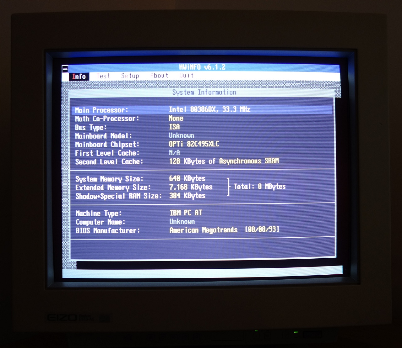
For some reason, the processor is detected as running at 35 MHz. But that is not true. The frequency counter says it's running at 33.33 MHz.


I stress tested the system for a couple of hours with various benchmark utilities and everything appears to be working as expected. No issues whatsoever. I also installed the NPU.

HWiNFO correctly detects the numeric processor. However, the NPU is reported as running 0.3 MHz faster than the CPU. While it's true that the NPU can (but in my case doesn't) run on an asynchronous clock (non buffered) mode, the frequency is actually the same for both CPU and NPU.
The only electrical difference of the synchronous clock (buffered) mode and the asynchronous clock (non buffered) mode is an additional 4 ns propagation delay introduced by the 74F08 master clock buffer IC on the NPU-CLK signal by means of JP8, pins 1-2, causing the CPU and NPU to run on a synchronized clock signal. Setting JP8, pins 2-3 will remove the additional propagation delay from the NPU clock transmission line, causing the CPU and NPU to run on asynchronous clock signals. For the record, this 4 ns delay is continuously coupled into the transmission line for the CPU-CLK signal and cannot be altered by jumpers.

However, all is not finished, yet. The JETkey keyboard controller is configured in AT-mode and I am using a two IC prototyping board connected with plain wires to the appropriate pins on IC32 socket. I have to solve this by either finding a different ROM BIOS image that accepts PS/2-mode keyboard controllers or patch the current ROM BIOS directly in HEX so that it will accept any controller version.
As always, let's take the hard way and try to understand what the ROM BIOS is doing and how I can patch it to fulfill the needs of the SBMC. I started a new topic under the Essays and Research category on the main Microelectronics page. Refer to the Adapting an 80386DX ROM BIOS for PS/2 Keyboard and Mouse Support article for more details.
In the meantime I have also sourced an American Megatrends AMI KB-BIOS-VER-F integrated circuit. Let's test this one for now.

Well, well, what do you know!? The AMI keyboard controller works hands-on in PS/2 keyboard mode. I can finally feel the taste of success. I can't vouch for the PS/2 mouse, yet. But I will test that as well.
At a later point in time, I have tested the PS/2 mouse and I can confirm that it is working either with the modified 8/8/93 AMI BIOS ROM image or MR-BIOS.
Now, let's insert a LIR2032 battery and observe the charging circuit.

It works correctly. The orange LED is lit while charging and the green one lights up when charging is complete. The SETUP data is now correctly kept in the non-volatile CMOS memory.
Just for the fun of it, I wanted to take a picture of the miniature bubble displays. Unfortunately, the camera angle and the color rendition of my old Sony camera just won't do them justice.

Here's the POST screen. One very interesting detail, is that the BIOS string now ends in -F. So, my initial assumption that the BIOS expects a keyboard controller with an H version is somewhat wrong. While it is true that it expects only a few selected keyboard controller versions, it is also true that it displays the said version within the BIOS string. That's an unexpected fact.
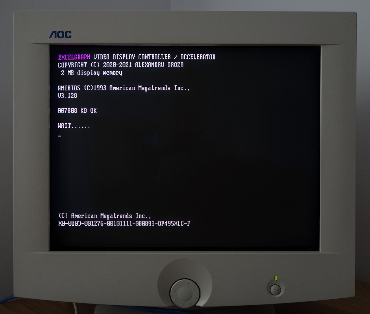
Finally I have installed 32 Mb RAM based on eight 4Mx9 70ns SIMM that I designed in the meantime.

Now, there is more than enough random access memory for any task that might be accomplished by this computer.

Booting to an MS-DOS commandline prompt. The AIF driver is loaded.

Here is an overview of the entire PCB assembly with all the parts installed in their respective sockets.

Looks good so far.
Going One Step Further
The fastest 386 processor would be a Texas Instruments TX486DLC/E-40GA part. There is an equivalent Cyrix processor but it is actually a rebranded Texas Instruments CPU. I will also use a small aluminum heat sink with this CPU. For this purpose, I am going to use a piece of double sided adhesive thermal transfer tape. As for the NPU, I will go with a Cyrix CX-83D87-40-GP part.

Like this.

Texas Instruments TX486DLC/E-40GA CPU and Cyrix CX-83D87-40-GP FPU are in position.

The small heat sink should cool down the CPU by around 10 °C.

Temperatures
For documentation purposes, I took some temperature measurements with a thermistor-based digital thermometer. While it is not as accurate as an infrared thermometer, it still shows the temperature of the various heat zones on the PCB assembly.
As for the test procedure, I just let the machine for one hour of running Doom demos. Next, I have recorded the following temperatures.
- Texas Instruments TX486DLC/E-40GA CPU with heat sink: 57 °C
- Cyrix CX-83D87-40-GP FPU without heat sink: 31 °C
- DM9368 with heat sink: 40 °C
All other chips are operating well under 30 °C.
I would say that a low-noise 80 mm Noctua cooling fan spinning at around 700-800 RPM would be useful to blow air on the entire SBMC assembly while using the 40 MHz TX486DLC/E-40GA CPU. Another idea would be to use a bigger heat sink to drop the CPU temperature to around 40 °C. My PC case actually has a very conveniently positioned 80 mm fan cutout on the front panel. Although I was not fully convinced, I have installed such a fan, after all.

Since the SBMC PCB is very long, the fan doesn't fit correctly on the metal fixture without interfering with the connection jumpers. Thus, I have used some hexagonal spacers to allow for the required clearance. Thankfully the frontal plastic mask is deep enough to allow for the width of the fan and the spacers.

The fan is a 12 V PWM model that I had around from an old PC. I am running it in non-PWM mode at a fixed 5 V provided by a dedicated header on the system backplane. The noise floor is minimal and the fan runs quieter than the power supply fan. The airflow is not great but it is sufficient to provide some extra cooling to the hot TX486DLC CPU.
Just like I recommended in the beginning of the article, I installed small heat sinks on each of two the 7-segment driver ICs. I used two pieces of double sided adhesive thermal transfer tape, each of them being the size of a 16-pin IC plastic package top section.

I think these ICs are still running too hot, even with the additional heat sinks. I would say there is room for improvement in this area. I am thinking about some additional current limiting resistors, one for each LED segment. I will address this small inconvenient in a future revision of the printed circuit board.
All right, time to wrap things up and put an end to this adventure, for now.
Known Issues
I have added this section after I successfully built and tested VER 1.8 REV. D PCB assembly. These known issues apply only to this specific system version and revision.
My initial tests revealed that the system is not working with the DMA transfers initiated by sound cards. At least, it is not working with my ISA Audio Interface and neither with an AZTECH 16 Sound Blaster clone card that I have around. Weird thing is that when the cards initiate digitized sound DMA data transfers, the system crashes completely and the CMOS NVRAM is filled with garbage data, leading to a corrupt CMOS checksum error. You have to either restore the CMOS contents or reenter the BIOS ROM Setup program and correctly set the parameters.
In addition, I have spotted floppy disk drive issues, which I believe are also DMA-related. If I try to boot the system from a floppy disk or even attempt to access the floppy disk from the MS-DOS prompt, the system hangs. In this case, CMOS NVRAM is not affected. But I still suspect a DMA problem.
I don't know what exactly causes this behavior but I will investigate it at some point and come back with the findings.
Martin L. from the Czechs Republic informed me that his 80386DX SBMC does exhibit the same known issues but they manifest themselves a bit different. The CMOS NVRAM is not affected and also he manages to obtain some kind of digitized samples from the audio cards. The floppy issues on his side are related to data integrity errors on both read or write. But in some cases, he managed to use the floppy disk drives without any issues at all. On the other side, he uses a different ROM BIOS image than what I initially used. Good to know, I will try that specific ROM BIOS as well.
I also plan to spend some time with the logic analyzer on my prototype PCBA and try to get some usable information after the data acquisition and analysis phase.
Approaching The End
I had a lot of fun designing this project and I learned a lot of interesting stuff. This knowledge will be very useful for all my next microcomputer related projects.
Now, comes my reward: I'm going to play Wolfenstein 3-D on my homemade 80386 computer. I feel like I'm in 1993 again. But this time, with self-made hardware. As a surprise, I found six totally new episodes for Wolfenstein 3-D designed by Thomas Weiling. I played them a bit and I can say they are on par with the originals. Or even better than some of the original maps. He also created new levels for Spear of Destiny. I will try those as well.
I have further observed that neither of my two sound cards won't work with this 80386 computer. FM music plays great but whenever the sound card initiates a DMA transfer, the machine hangs completely and the CMOS NVRAM is overwritten with garbage data. Thus, no digitized sounds for now. I will investigate this issue. In the meantime I have just added a Known Issues section.
Final Conclusions
This project enabled me to dig deeper into the x86 platform system design and impulsed me to create all the other PC ISA cards required for a complete early '90s computer. I learned things, I faced failures, disappointments, sadness, successes, happiness, and other mixed feelings.
In terms of electronics workshop, I made the transition from a simple 2 x 100 MHz analogue oscilloscope to a 2 x 250 MHz digital one. Finally, I upgraded to a logic analysis mainframe equipped with four individual 110 MHz state / 500 MHz timing LA cards and a dual channel 500 MHz digital sampling oscilloscope card. In fact, this thing was cheaper and occupies less bench real estate than my former two oscilloscopes. Which I sold anyway to finance the 25 kg mammoth.
I wouldn't even have had any chance to debug the microcomputer card without the help of a logic analyzer. Actually, the logic analysis system repair and maintenance was kind of a big side project of its own. But all the work I did on it had already paid off. It took me literally five minutes with the logic analyzer to figure out what the problem was with the keyboard controller.
Needless to say that my reverse engineering skills improved greatly and I learned about other cool stuff such as inverse assemblers and hardware level microcode sniffing. In addition, I acquired a new skill by learning to operate the logic analyzer.
Overall, the time I invested into this project was well spent. And I believe I finally reached the end of this long article.
Constructing a Second 80386DX SBMC
This 80386DX subject just doesn't seem like willing to end. Which is not such a bad thing after all. As long as I am having fun or learning new stuff, I will also document my research and findings.
Apparently, this project generated some interest within the retrocomputing community and some people even managed to construct this microcomputer based on the Gerber files and the schematic diagram. That was unexpected! Like any other system design related project on my site, this one was initially intended for personal use only. But since a lot of people contacted me regarding this design, I decided to attach the Gerber files for download. And so I did with the rest of the system design projects. While it's no easy task, you can now venture into assembling your own 80386DX CPU card.
One thing is for sure: this project is not for sale. If you paid money then I just hope you didn't paid more than the cost of individual PCB and components. Otherwise, you have been scammed. But let's leave that away for a while.
One of the retrocomputing enthusiasts from the Czechs Republic, placed a bigger order at JLCPCB for some 80386DX SBMC printed circuit boards. And he sent me a couple of them, free of charge. I still have a couple of purple PCBs from OSHPark and now I have two additional green ones from JLCPCB. I recently did a side by side comparison between the JLCPCB and the OSHPark printed circuit boards. Refer to the 80386DX SBMC - OSHPark vs. JLCPCB article for more details.
For now, I decided to construct a second 80386DX ISA card with one of the PCBs that I received from Martin -- thanks, by the way.
Now, what was the formulation? Ah, yes: Here we go again!
First, I will recover all usable parts from the dead VER 1.6 REV. C prototype printed circuit board. And by all I mean all parts, even the carbon resistors. Since I already have the majority of the required parts, I thought I might as well just use them. Even if that implies some considerable desoldering effort.
Recovering parts is a tedious job but I have a lot of experience. In the past, I used to do this on a daily basis. I was scavenging discarded PCBs and then I was extracting the parts that were useful for my projects. I have some fond memories of those times. However, these days I'm using an electronic vacuum desoldering station which makes things a lot easier than my old mechanical pump.
This is the green PCB, components side.

And the solder side.

Versions and Revisions
This section lists the project version and revision history.
VER. 1.8 REV. E
- Replaced IC25 from 74LS04 to 74ALS04
- Renamed some signals for consistency
- Corrected double pull-up of SA12 signal
- Minor PCB routing improvements
VER. 1.8 REV. D
- Fully functional production version
- Various schematic-level improvements and renaming of signals
- Internal ground and supply planes doubling as high-speed AC signal return paths
- All signal tracks are routed exclusively either on top (1) or bottom (4) layers
- Shortened signal tracks wherever possible
- Reduced number of vias
- Corrected /XIOR and /XIOW signal connections
- Corrected port 80h diagnostics address decoder
- Improvements to master clock generator circuit and clock transmission lines
- Implemented a proper lithium-ion battery charger circuit
- Added more decoupling capacitors targeting different frequencies in key positions
- Various silkscreen updates
VER. 1.6 REV. C
- Non-functional initial prototype version
Copyright © 2004- Alexandru Groza
All rights reserved.
VER. 1.0 | REV. A